
Creating an SWD Adapter for STM32 Development Boards (Part 2)
In the last post, we started to look at how we could design a simple programming adapter for STM32 development boards. We walked through the process necessary to get the schematics completed. In this post, we will examine the the PCB layout along with the BOM and costs necessary to prototype this simple board.
With the schematics completed, the components and nets are pushed into the PCB document literally with the press of a button. There’s not much there. Literally three components with nets that are ready to be routed. I don’t want to spend too much time talking through PCB layout since it’s really beyond the scope of these posts. With that in mind, here are a few bullets on the process that I follow when laying out the board.
- Arrange the components on the blank sheet
- Auto-route to make sure that there is a valid routing solution
- Define the board outline (in this case ~1 inch by 0.75 inches)
- Route any power signals (VCC, etc)
- Set the strategy for return paths and grounds
- Route the signals
- Add polygon fills
- Add copyrights, notes, etc
- Review the layout
- Make any adjustments
- Generate production documents
I will point out that during the components arrangement phase it can be critical to make sure the connectors are in the right direction. The best thing you can do is physically hold and look at the cables. I actually laid this board out and then afterwards found the cable I was going to use. Guess what? Yea, I had P2 rotated 180 degree in the wrong direction! I could have made it work but it turned out that rotating it cleaned up the layout. Just look for yourself at the following top and bottom layers:
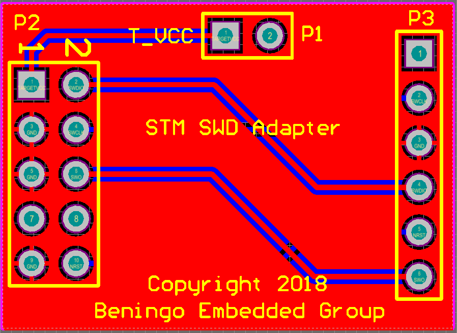
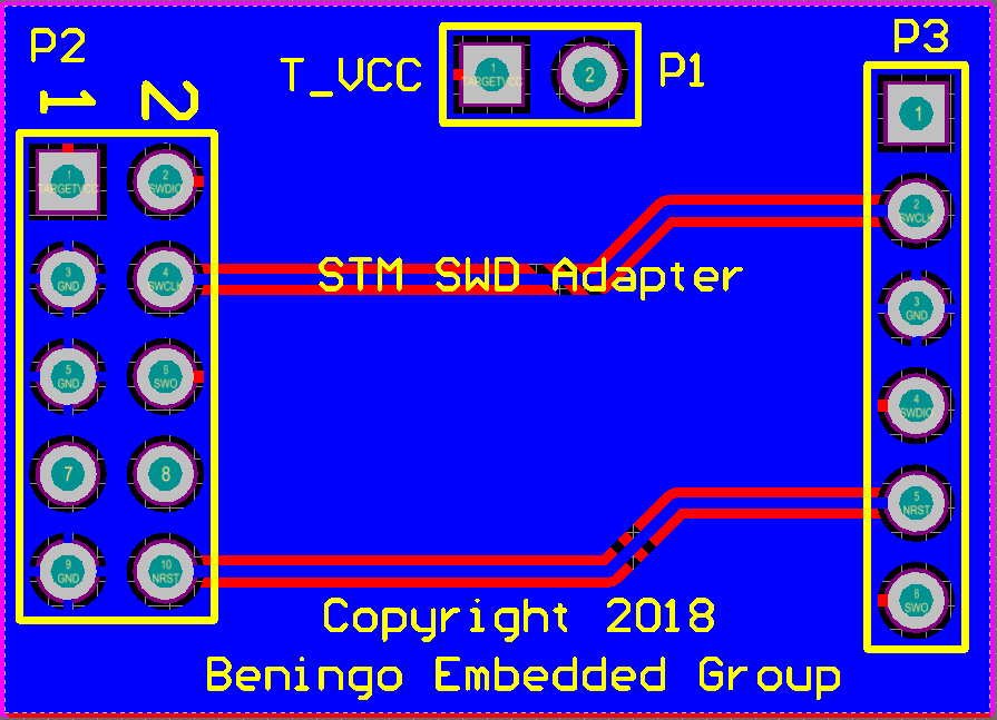
As you can see, using two layers, routing these signals is very easy and was possible without having to add any vias!
One thing I always like to do when designing a board is to look at the generated board on how it is supposed to look in a 3D rendering. When doing this, it’s possible to add in 3D models for the connectors which can then be exported for mechanical engineers to build housings and other work with the electronics model. For this simple board, I didn’t spend the time to add those connector models in. I was still able to look at how the board would look though, which is below:
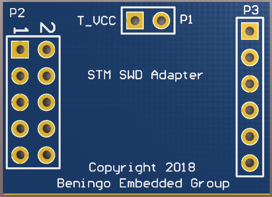
In this model, we are looking at the top layer. On the left, the 10 pin connector would be mounted on the top along with the two pin, male connectors. P3, which is a female connector that connects to the target, will actually be placed on the bottom of the board.
The bill of materials (BOM) for the board is also really simple. I chose the following components for my board:
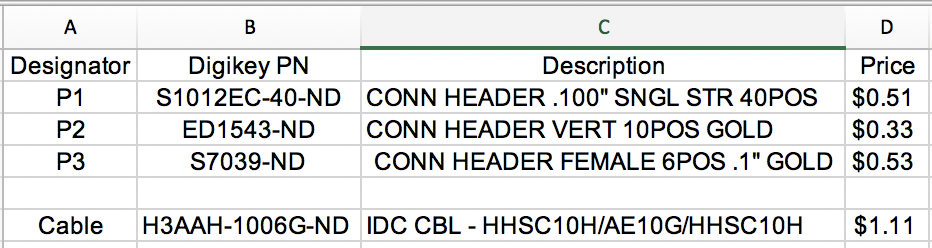
There are several things to note here:
- Component P2 could be very different for developers depending on the cabling that they use on the programmer. I chose to use old school IDC connectors.
- The connector BOM cost is not more than $1.50.
- I added a IDC cable, just in case I didn’t have one, to connect the external programmer to the adapter board.
- The pricing for the PCB is not listed here.
As it turns out, the PCB cost is the largest expense if you are doing a small board run. I poked around and found that for ~$100, including shipping, I could build around 50 boards. This is great if you are planning to manufacture these devices but I really only had interest in building 5. So overall, each adapter will cost me around $25 which is well worth the investment to clean-up the way that I’m interfacing to a development kit.
Could I have done this cheaper? Absolutely! I could have just purchased several $1.11 cables, cut off the connector and then directly soldered the cabling onto the P3 connector. I would still need to add the VCC jumper, but some nice cabling could have been built for probably $5 plus some time at the soldering iron. But let’s be honest, that’s not as fun as laying out a board.
I hope that these two posts have given you some ideas on how you can interface an external programmer to the STM32 development boards. Obviously these ideas could easily be applied to any vendors development boards.
Struggling to keep your development skills up to date or facing outdated processes that slow down your team, raise costs, and impact product quality?
Here are 4 ways I can help you:
- Embedded Software Academy: Enhance your skills, streamline your processes, and elevate your architecture. Join my academy for on-demand, hands-on workshops and cutting-edge development resources designed to transform your career and keep you ahead of the curve.
- Consulting Services: Get personalized, expert guidance to streamline your development processes, boost efficiency, and achieve your project goals faster. Partner with us to unlock your team's full potential and drive innovation, ensuring your projects success.
- Team Training and Development: Empower your team with the latest best practices in embedded software. Our expert-led training sessions will equip your team with the skills and knowledge to excel, innovate, and drive your projects to success.
- Customized Design Solutions: Get design and development assistance to enhance efficiency, ensure robust testing, and streamline your development pipeline, driving your projects success.
Take action today to upgrade your skills, optimize your team, and achieve success.


Thanks for a nice writeup.
After having to digest all this information on my own, I decided to adopt TagConnect TC2030 connector-less adapters in my designs. It is great for PCB prototypes because it uses needles which take almost no space on custom PCBs. Using TC2030-NL (no lead) cable version, future manufacturing process allows fast and painless batch programming. It is investment in the start, but it pays off in the long run.
After seeing how much similar adapters cost, I even made my own “Cortex-M JTAG Interface Extender” board with JTAG-20 IDC connector on programmer side and RJ12 connector for TC2030 cable on the target side, plus some extras. I am using it with J-Link and external genuine STLink programmers.
Thanks for the comment. I love the TagConnect adapters! I use them as well on as much as possible. I only wish that ST Microelectronics had put them on their development boards!
Yes, the 20 (2×10) IDC pin standard solution is slightly too big for modern designs, and a half of pins are just for GND (probably designed for longer cables: GND @ every other line as a result of the pin layout may probably help to eliminate crosstalk between them).
Smaller connectors designed for shorter cables may /shall work equally well.
But an issue shows up: there is a need (a lack of a) standard pinout, so application engineers can buy those $2 solutions rather reinvent a wheel (a time to figure it all out and put it into a practice costs hundreeds of $…).
Following all-in-one adapter exists, but its CPU side (e.g. the ARM 2×5 pin socket) might still be smaller… : https://abc-rc.pl/adapter-wielofunkcyjny-jtag Additionally, I see no SWO line there (while STM promotes this for a printf style of a debugging)…
Would following pinout (a subset of pins) make sense for STM32F4 (in system programming & debigging)?:
9)JTAG_JTCK_SWCLK GND (10
7)JTMS_SWV_SWDIO GND (8
5)JTAG_JTDI JTDO_SWO (6
3)NJRST NRST (4
1)3V3 3V3 (2
Would T821110A1S100CEU (2×5 pin IDC) connector serve for the purpose, or there would be better industry standard options aroud ?
Thanks for the comment! They are very big for todays designs but unfortunately quite a few Debuggers/Programmers still use them. It then becomes a challenge to find an existing adapter sometimes, which drove this post.
On any of these you definitely want to make sure that the SWO line is available. That trace line is so important for debugging.
The pin-out you mention looks similar to what I had done but again, it may depend on the exact board or setup that you have in your lab.
I’m also pretty bad at connectors so while the T821110A1S100CEU looks like it would work, I would buy one just to test it. I ended up doing that for my setup. Still waiting on my PCB’s to test ….
Hi Jacob,
Where did you end up getting your PCBs made?
Thanks!
This time I used a place called PCBcart. I used to have them do my prototype boards several years ago because the quality was good and the boards were inexpensive. This time though, quality was good but the cost was much higher. I’ll be posting a blog soon on several quick turn prototype PCB houses that developers can use.
Thank you, Jacob.
That would be a very helpful list of PCB houses too.