
Simple Tricks to Minimize “Crossed-Wire” PCB Rework
One of the most common issues I see with schematic and PCB layout is crossed wires. For example, the designer has connected the USART peripherals transmit line to the transmit line of the receiving device instead of the receiving line. The designer thought they had it right, but maybe each device specified what Tx and Rx mean from a different perspective. Given two choices, Murphy’s Law guarantees that we will select the wrong choice 100% of the time. This post will explore a few PCB tricks that designers can use to recover from a crossed wire error.
Cutting and careful soldering
When we discover that we’ve swapped the Tx/Rx or the CTS/RTS lines, we know 100% that we will have to go back and rework the PCB artwork to make it right. In the meantime, the electrical engineers and the software developers will need those boards for testing. I typically see designers assuming that they will get it right on the first try. With a wrong assumption, the designer or board house is going to be forced to follow an annoying procedure which includes:
- Scrapping the solder mask off the offending traces
- Carefully cutting the offending traces to break their electrical connection
- Soldering jumper wire from the first exposed trace to the other exposed trace
- Repeating step 3 for the other trace pair
While this will fix the electrical connections, the result is a franken-board that is delicate and prone to failure.
Designers should lay out their board with the expectation that there will be errors; after all, we are only human. Let’s now examine two tricks to make reworking such errors easy.
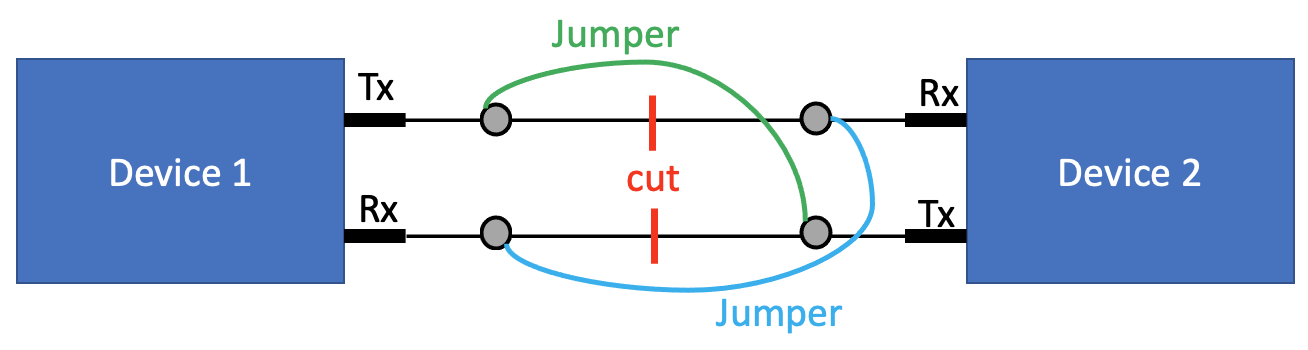
PCB Trick #1 – Include two vias on each trace
The first trick designers can use is to include two vias on each trace, as shown in Figure 1. The vias provide two advantages here. First, it gives a prominent place to cut the trace to severe the connection between the two devices. Second, the vias act as a perfect place to solder wires! We can use rework wire and solder it into the two vias, assuming we’ve sized them properly. The time required for the rework is minimal, and the board fix is much more robust. While we know the software developers will still probably break the wires somehow, it should take them longer, and when they do, the repair is simple since it won’t be a broken trace.
Figure 1 – Include two vias on each trace to ease cutting and jumpering crossed-wire errors.
PCB Trick #2 – Use an inline resistor
Using a couple of vias is a reasonable solution, but I don’t like having to cut traces on the board. I also don’t like having to add extra holes in the PCB, partially because it can increase the board cost. (Although, honestly, the cost increase is minimal, and it does provide extra test points for debugging, which is always beneficial). If I’m laying out a PCB, I will add inline resistors on traces, as shown in Figure 2.
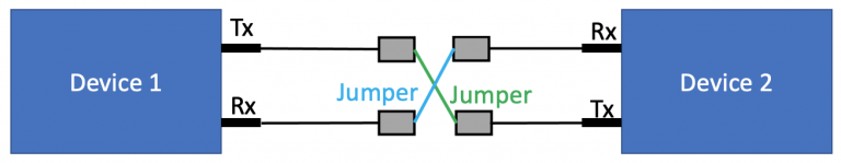
Figure 2 – Using an inline resistor quickly provides a pre-cut trace and pads to solder jumper wires.
If the designer didn’t make any mistakes laying out the board, they would populate a $0.001 0-ohm resistor. However, if there is a mistake, the board is set up to resolve the issue in just a few minutes.
The inline resistor trick is essentially the same idea behind the multiple via trick, except that we have less work! The pads for the inline resistors automatically “cut” the trace for us. The pads also provide an excellent soldering point to solder jumper wires to the right connections! Again, I would recommend tacking down the soldered wires to prevent any stress from lifting the pads off the board and damaging it.
Conclusions
Schematic and PCB errors are bound to happen. No matter how much experience you have, there will be an issue at some point. Rather than assume that we will get it right on the first try, plan for errors. Crossed wire issues with Tx/Rx and RTS/CTS pairs can easily be fixed on prototype boards with minimal rework by using either inline resistors or adding a few extra vias to the traces. You’ll be glad you thought ahead when you have a dozen boards that need to be reworked.
Struggling to keep your development skills up to date or facing outdated processes that slow down your team, raise costs, and impact product quality?
Here are 4 ways I can help you:
- Embedded Software Academy: Enhance your skills, streamline your processes, and elevate your architecture. Join my academy for on-demand, hands-on workshops and cutting-edge development resources designed to transform your career and keep you ahead of the curve.
- Consulting Services: Get personalized, expert guidance to streamline your development processes, boost efficiency, and achieve your project goals faster. Partner with us to unlock your team's full potential and drive innovation, ensuring your projects success.
- Team Training and Development: Empower your team with the latest best practices in embedded software. Our expert-led training sessions will equip your team with the skills and knowledge to excel, innovate, and drive your projects to success.
- Customized Design Solutions: Get design and development assistance to enhance efficiency, ensure robust testing, and streamline your development pipeline, driving your projects success.
Take action today to upgrade your skills, optimize your team, and achieve success.


What you don’t mention, thou You do hint at under trick #2, is that wen the serial line is giving issues, one of the first thing we do anyway is to solder small wire stumps to connect a probe for the scope.
So adding the via’s or resistors also help on the debugging even if the bug is in the SW.
+1 for providing testpoints. On one project, we had to a scope probe to a 5mm LED under software control as that was the closest thing to a testpoint.
Yikes! Test points are definitely critical to being able to debug. I often drive the younger engineers I work with crazy because I constantly ask them about test points, spare GPIO, and other items that make debugging so much easier.
Most MCUs allow mapping of peripheral functions to pins. In particular, the Nordic nRF52 allows almost any function to be mapped to almost any pin. Simply remapping fixed a crossed wire problem I recently had.
Thanks for the comment!
Definitely! Just remapping pins is a potential solution, provided your MCU supports it. Unfortunately, not all MCU’s have adopted a multiplexing scheme where any function can be mapped to any pin. I definitely agree this is the easiest if supported!
Test points can help with QA also. I have a few Arduinos with relay hats for actuating switches and overriding thermistors and switching charging on and off, and I use them to build unattended tests.
Another tip – Since connectors are a huge issue (Still), route traces to through hole connectors on the outside layers to make fixes easy. Where applicable naturally. Like Serial Connectors, Programming plugs, etc.
We do design reviews of all schematics before releasing the PCB for fabrication. We typically catch most errors by doing that. But that only works when you have … er … retentive engineers who are extremely picky, as well as designers who are willing to listen to the ramblings of said picky reviewers. And always run the design rule checker on the PCB layout. Always.
I am 100% with you on test points. I’ve worked on boards with them and boards without them, and I definitely prefer having test points over asking one of the EEs to add patch wires to a 0.1″ header that I can connect to my logic analyzer.
At my first job, on uart with an external board we used a special footprint to allow us to switch RX/TX without any wire.
|——-|
—-A B-| C
|—————-
——-D E————-
By defaut you populate AB and DE but if you want to switch you do BD and CE
|——–|
—-A B-| C
|—————-
———D E————-
(Better with good spacing)
You refer to ‘tacking down’ any wires soldered to the PCB. I often use a blob of hot melt glue or 2-part epoxy to protect/cover/retain delicate board fixes, making the board very robust for subsequent handling – even sufficient for field use. It can also help to secure fine test wires that go off the board to other equipment.