
Creating an SWD Adapter for STM32 Development Boards (Part 3)
My adapter boards have arrived! As we discussed in the first two parts, the on-board debugger that comes with most development boards is functional but often offers far less than a professional debugger. We’ve been exploring how we can create an adapter board for the ST Microelectronic development boards that will allow us to use an external debugger easily. In today’s post, we will examine the final results!
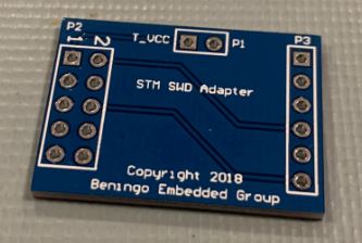
After opening up and examining my boards, I found that they appeared to be in good shape. As you can see below, the board looks just like what we laid out in part 2 and measured around 1 inch by 1.25 inches:
After firing up my soldering iron, I soldered my components onto the board. The JTAG/SWD and my power pins on top, the 6-pin SWD on the bottom. The assembled board can be seen below:
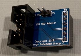
At this stage, I noticed two minor defects:
- I never measured the JTAG/SWD connector size so the connector was slightly wider than the board
- The JTAG/SWD connector was wide enough that it covered some of the silkscreen for VCC and my company name
Neither of these defects affects the way that the adapter would operate in the slightest. Given how quickly I put this board together and how I just guessed at the board size, I was pretty happy with the way the board turned out. In fact, these defects are so minor that if I didn’t point them out, they would probably not even be noticeable.
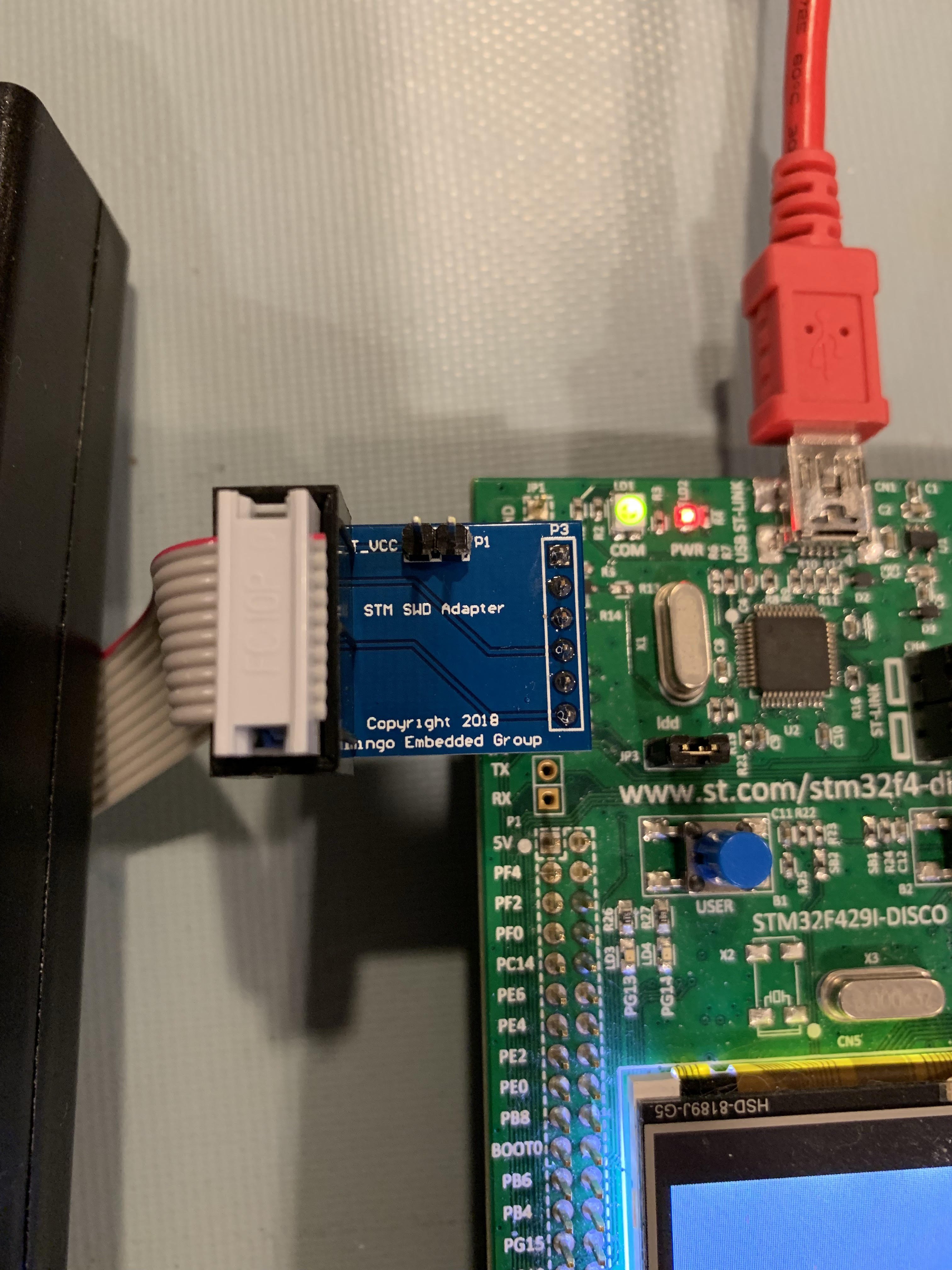
With the board assembled, it was time to test it out and see if I could actually program a microcontroller with my adapter. For the test, I connected my adapter board to the 6-pin connector on the STM32F429I-Discovery board. I also connected a 20-pin to 10-pin IDC connector to my SEGGER J-Link Ultra+ and connected my new ribbon cable to the adapter board. At this stage, the setup looked as follows:
If you remember back, I had to put the VCC pin on the board in order to detect if the target MCU was powered. At this point, we need to jumper the VCC pin on the adapter board to the VCC on the development board. In order to do so, I used a Sparkfun female-to-female adapter and connected to one of the of the 3V pins on the STM32429I-Discovery board. The final setup can be seen below:
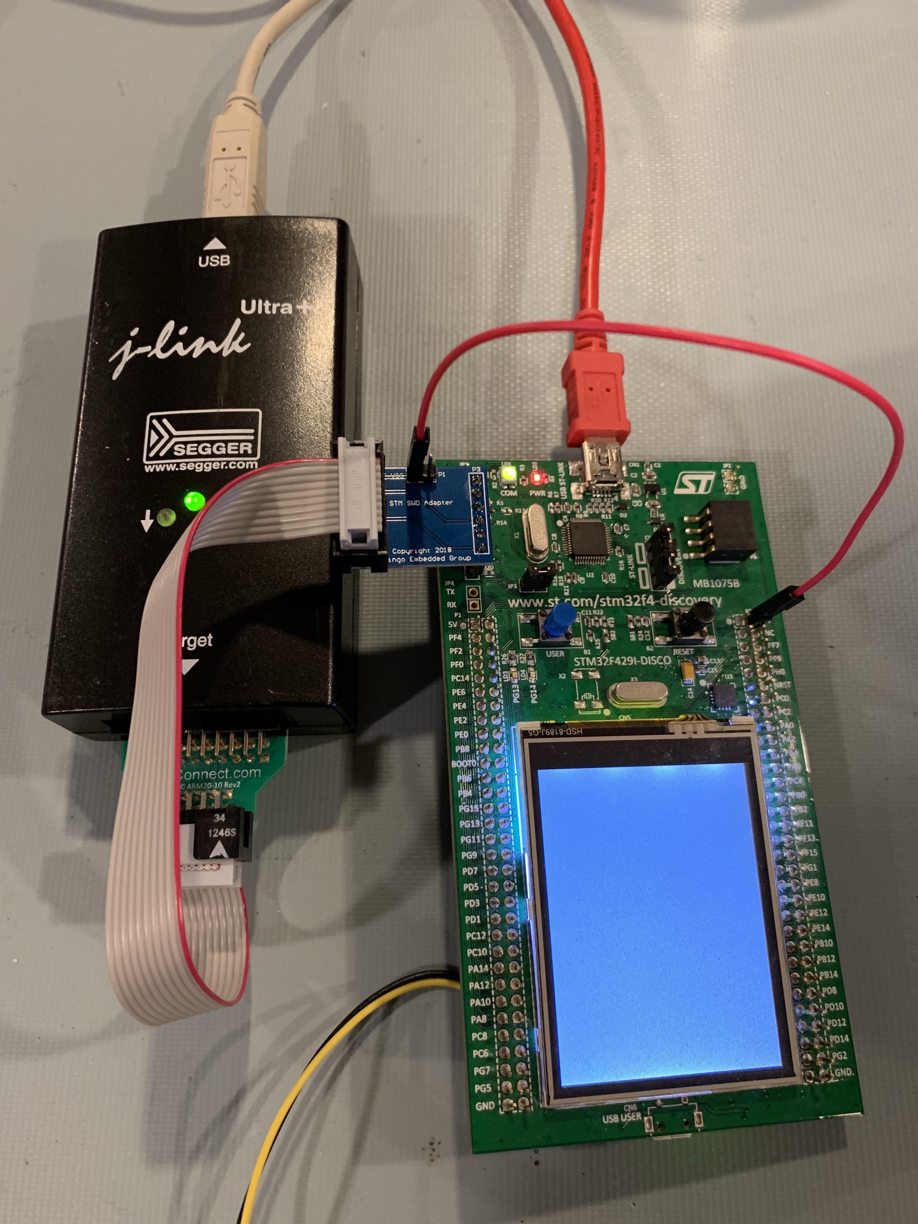
The real test of course was whether I could program the microcontroller. I connected the J-Link to my PC and attempted to program the board using a simple RTOS LED blinky program. Thankfully, everything worked as expected! No more jumper wires for me! (Well, just the one anyways for VCC).
If you are interested in downloading the design files and gerbers that I used for this project, you can find them below.
DISCLAIMOR: By downloading these files, you contractually agree that:
THESE FILESS ARE PROVIDED BY BENINGO EMBEDDED GROUP, LLC “AS IS” AND ANY EXPRESSED OR IMPLIED WARRANTIES, INCLUDING, BUT NOT LIMITED TO, THE IMPLIED WARRANTIES OF MERCHANTABILITY AND FITNESS FOR A PARTICULAR PURPOSE ARE DISCLAIMED. IN NO EVENT SHALL BENINGO EMBEDDED GROUP, LLC OR ITS CONTRIBUTORS BE LIABLE FOR ANY
DIRECT, INDIRECT, INCIDENTAL, SPECIAL, EXEMPLARY, OR CONSEQUENTIAL DAMAGES (INCLUDING, BUT NOT LIMITED TO, PROCUREMENT OF SUBSTITUTE GOODS OR SERVICES; LOSS OF USE, DATA, OR PROFITS; OR BUSINESS INTERRUPTION) HOWEVER CAUSED AND ON ANY THEORY OF LIABILITY, WHETHER IN CONTRACT, STRICT LIABILITY, OR TORT (INCLUDING NEGLIGENCE OR OTHERWISE) ARISING IN ANY WAY OUT OF THE USE OF THESE FILES, EVEN IF ADVISED OF THE POSSIBILITY OF SUCH DAMAGE.
Struggling to keep your development skills up to date or facing outdated processes that slow down your team, raise costs, and impact product quality?
Here are 4 ways I can help you:
- Embedded Software Academy: Enhance your skills, streamline your processes, and elevate your architecture. Join my academy for on-demand, hands-on workshops and cutting-edge development resources designed to transform your career and keep you ahead of the curve.
- Consulting Services: Get personalized, expert guidance to streamline your development processes, boost efficiency, and achieve your project goals faster. Partner with us to unlock your team's full potential and drive innovation, ensuring your projects success.
- Team Training and Development: Empower your team with the latest best practices in embedded software. Our expert-led training sessions will equip your team with the skills and knowledge to excel, innovate, and drive your projects to success.
- Customized Design Solutions: Get design and development assistance to enhance efficiency, ensure robust testing, and streamline your development pipeline, driving your projects success.
Take action today to upgrade your skills, optimize your team, and achieve success.


Great to see it’s alive and works. Congratulations!
Here comes a question though: would you be able to enlist functionalities you see as working, and what looks to be missing, or works but slighty slower with this particular set of 6 pins e.g. comparing to 20-pin ARM JTAG standard?
I mean e.g.: SWO printf based debugging, pausing and stepping through a code, mem watches, profiling (e.g. from Atollic True Studio or simmilar), variable watching from STM Studio, basic mem read-write operations (e.g. from SMT32 ST-Link Utility)?
It looks codeload does work. Does it also reset a target after codeload (start the code) w/o a need of pressing the phisical reset button on the target (ST discovery) board?
How about a speed (e.g. when writing or reading a content of a flash)?
I know there are many questions here (some answers will probably come with a time), but even a partial info/response will bring a value.
Thank you Jacob in advance for sharing your experiances on the matter.
The on-board debuggers are very limited. They are designed to be a minimal solution to program a microcontroller. If you look at the datasheet, the connection speed is something like 15 kb/s on the ST-Link v2 versus 1 mb/s on the J-Link EDU. Far faster speeds are available on the higher end debuggers.
Everything is faster using an external programmer through this adapter interface. There are also improvements based on the probe used such as unlimited break-points, the ability to access multiple buses simultaneously and so on.
I will put it on my list to write a blog that compares a “stock” debugger with what I consider to be a “professional” debugger in a future post. Thank-you for the questions!
🙂